FPGA 版 FM 音源 (63) -- FPGA 版 EG (7)
EG モジュールのトップレベル回路図「opl3_EG_top.bdf」を下に示します。 (図をクリックすると拡大します)
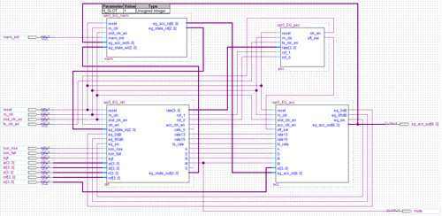
この回路は、下位モジュール同士の結線自体は 2017 年 1 月 23 日の記事の回路 (→こちら) と同じですが、入出力ピン数削減のため、出力を EG アキュムレータ出力の 9 本と、ミュート状態出力の 1 本に限ったものです。
この回路図ファイル (opl3_EG_top.bdf) を Quartus II のメニューから
File → Create / Update → Create HDL Design File from Current File... → Verilog HDL
と選んで機械的に Verilog に変換されたファイルに、一部、手を加えたものを下に示します。
"opl3_EG_top.v"
// Copyright (C) 1991-2011 Altera Corporation
// Your use of Altera Corporation's design tools, logic functions
// and other software and tools, and its AMPP partner logic
// functions, and any output files from any of the foregoing
// (including device programming or simulation files), and any
// associated documentation or information are expressly subject
// to the terms and conditions of the Altera Program License
// Subscription Agreement, Altera MegaCore Function License
// Agreement, or other applicable license agreement, including,
// without limitation, that your use is for the sole purpose of
// programming logic devices manufactured by Altera and sold by
// Altera or its authorized distributors.  Please refer to the
// applicable agreement for further details.

// PROGRAM		"Quartus II"
// VERSION		"Version 11.0 Build 208 07/03/2011 Service Pack 1 SJ Web Edition"
// CREATED		"Mon Jan 23 08:03:05 2017"

module opl3_EG_top(
	reset,
	m_clk,
	slot_clk_en,
	fs_clk_en,
	kon_rise
	kon_fall,
	egt,
	mem_init,
	ar,
	dr,
	rof,
	rr,
	sl,
	mute,
	eg_acc_out
);

parameter  N_SLOT = 1;

input wire	reset;
input wire	m_clk;
input wire	slot_clk_en;
input wire	fs_clk_en;
input wire	kon_rise;
input wire	kon_fall;
input wire	egt;
input wire	mem_init;
input wire	[3:0] ar;
input wire	[3:0] dr;
input wire	[3:0] rof;
input wire	[3:0] rr;
input wire	[3:0] sl;
output wire	mute;
output wire	[8:0] eg_acc_out;

wire	SYNTHESIZED_WIRE_0;
wire	SYNTHESIZED_WIRE_1;
wire	SYNTHESIZED_WIRE_2;
wire	SYNTHESIZED_WIRE_3;
wire	SYNTHESIZED_WIRE_4;
wire	SYNTHESIZED_WIRE_5;
wire	SYNTHESIZED_WIRE_6;
wire	SYNTHESIZED_WIRE_7;
wire	SYNTHESIZED_WIRE_8;
wire	[8:0] SYNTHESIZED_WIRE_9;
wire	SYNTHESIZED_WIRE_10;
wire	SYNTHESIZED_WIRE_11;
wire	SYNTHESIZED_WIRE_12;
wire	SYNTHESIZED_WIRE_13;
wire	[2:0] SYNTHESIZED_WIRE_14;
wire	[8:0] SYNTHESIZED_WIRE_15;
wire	[2:0] SYNTHESIZED_WIRE_16;
wire	SYNTHESIZED_WIRE_17;
wire	SYNTHESIZED_WIRE_18;
wire	[3:0] SYNTHESIZED_WIRE_19;

assign	mute = SYNTHESIZED_WIRE_8;
assign	eg_acc_out = SYNTHESIZED_WIRE_15;


opl3_EG_acc	b2v_acc(
	.reset(reset),
	.m_clk(m_clk),
	.slot_clk_en(slot_clk_en),
	.acc_clk_en(SYNTHESIZED_WIRE_0),
	.sft_sel(SYNTHESIZED_WIRE_1),
	.rate13(SYNTHESIZED_WIRE_2),
	.rate15(SYNTHESIZED_WIRE_3),
	.hi_rate(SYNTHESIZED_WIRE_4),
	.A(SYNTHESIZED_WIRE_5),
	.D(SYNTHESIZED_WIRE_6),
	.R(SYNTHESIZED_WIRE_7),
	.M(SYNTHESIZED_WIRE_8),
	.eg_acc_in(SYNTHESIZED_WIRE_9),
	.sl(sl),
	.eq_0dB(SYNTHESIZED_WIRE_11),
	.eq_95dB(SYNTHESIZED_WIRE_12),
	.eq_slx(SYNTHESIZED_WIRE_13),
	.eg_acc_out(SYNTHESIZED_WIRE_15));


opl3_EG_ctrl	b2v_ctrl(
	.reset(reset),
	.m_clk(m_clk),
	.slot_clk_en(slot_clk_en),
	.clk_en(SYNTHESIZED_WIRE_10),
	.eq_0dB(SYNTHESIZED_WIRE_11),
	.eq_95dB(SYNTHESIZED_WIRE_12),
	.eq_slx(SYNTHESIZED_WIRE_13),
	.kon_rise(kon_rise),
	.kon_fall(kon_fall),
	.egt(egt),
	.ar(ar),
	.dr(dr),
	.eg_state_in(SYNTHESIZED_WIRE_14),
	.rof(rof),
	.rr(rr),
	.rof_1(SYNTHESIZED_WIRE_17),
	.rof_0(SYNTHESIZED_WIRE_18),
	.acc_clk_en(SYNTHESIZED_WIRE_0),

	.rate13(SYNTHESIZED_WIRE_2),
	.rate15(SYNTHESIZED_WIRE_3),
	.hi_rate(SYNTHESIZED_WIRE_4),
	.A(SYNTHESIZED_WIRE_5),
	.D(SYNTHESIZED_WIRE_6),
	.R(SYNTHESIZED_WIRE_7),
	.M(SYNTHESIZED_WIRE_8),

	.eg_state_out(SYNTHESIZED_WIRE_16),
	.rate(SYNTHESIZED_WIRE_19));


opl3_EG_mem	b2v_mem(
	.reset(reset),
	.m_clk(m_clk),
	.slot_clk_en(slot_clk_en),
	.mem_init(mem_init),
	.eg_acc_wr(SYNTHESIZED_WIRE_15),
	.eg_state_wr(SYNTHESIZED_WIRE_16),
	.eg_acc_rd(SYNTHESIZED_WIRE_9),
	.eg_state_rd(SYNTHESIZED_WIRE_14));
	defparam	b2v_mem.N_SLOT = N_SLOT;


opl3_EG_psc	b2v_psc(
	.reset(reset),
	.m_clk(m_clk),
	.fs_clk_en(fs_clk_en),
	.rof_1(SYNTHESIZED_WIRE_17),
	.rof_0(SYNTHESIZED_WIRE_18),
	.rate(SYNTHESIZED_WIRE_19),
	.clk_en(SYNTHESIZED_WIRE_10),
	.sft_sel(SYNTHESIZED_WIRE_1));


endmodule
手を加えた部分は、具体的には
parameter N_SLOT = 1;
の 1 行を追加したのと、
defparam b2v_mem.N_SLOT = 1;
を
defparam b2v_mem.N_SLOT = N_SLOT;
に書き換えて、トップレベルの opl3_EG_top() に渡した N_SLOT パラメタが下位モジュールの opl3_EG_mem() に渡るようにしたものです。